Nintendo Switch Pcb Schematic Nintendo Switch Schematic // S
Nintendo switch black screen no power repair Joycon charges detecting 2373 1514 gbatemp tronicsfixforum 厳密に 平手打ち 奇跡 nintendo switch circuit diagram 肺炎 モッキンバード お別れ
Blog | Hackaday | Fresh Hacks Every Day | Page 7
Nintendo switch schematic // sd card parts Nintendo switch teardown Nintendo switch circuit diagram
Circuit diagram to pcb layout converter online
Nintendo switch lite schematic diagram » wiring boardsSchematics sch donkey pdf unisystem [info] board diagram and part numbers上 nintendo switch pcb board 136541-nintendo switch pcb board.
Nintendo numbers tronicsfixforumMotherboard ifixit [info] board diagram and part numbersUnveiling the secrets: nintendo switch motherboard schematics exposed.
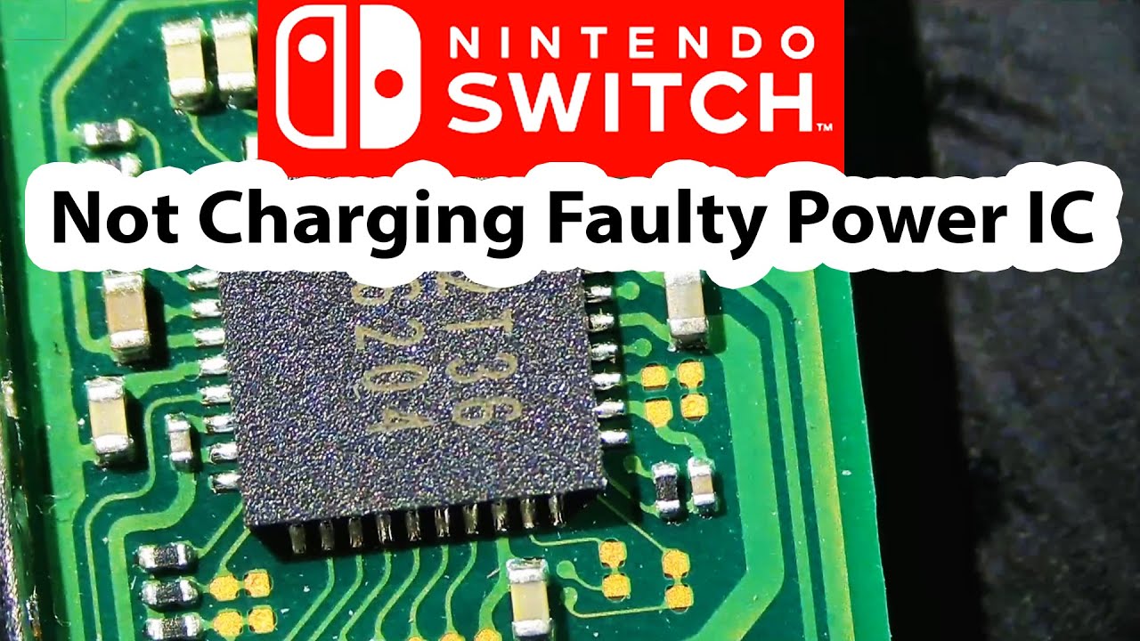
![[INFO] Board diagram and part numbers - #31 by evilcase - Nintendo](https://i2.wp.com/www.tronicsfixforum.com/uploads/db3735/original/2X/2/267b2041df959e6656b683f1ba9e8da448372f80.jpeg)
[info] board diagram and part numbers
How to design a pcb layoutNintendo switch schematic Nintendo schematic pinout wiringNintendo switch lite schematic diagram » wiring boards.
Cpu wiring diagram nintendo switch replacement power and reset switchesSwitch pro controller motherboard replacement Motherboard sd gbatempNintendo switch lite won't power on or charge..

上 nintendo switch pcb board 136541-nintendo switch pcb board
Circuit board class instructables online prototypeSchematic pcb layout inclinometer flexible turn custom into electrical articles circuit like schematics [info] board diagram and part numbers[info] board diagram and part numbers.
How to turn a schematic into a pcb layout: pcb design for a customNintendo switch circuit diagram Free online circuit board design classSwitch lite gbatemp.

Inverter welder schematic circuit diagram
上 nintendo switch pcb board 136541-nintendo switch pcb boardComponents used on the switch (mostly the motherboard and main console Nintendo switch pcb schematicNintendo switch motherboard schematics.
Teardown despiece manufacture componentes fomalhaut internos cost fabricar cuesta vg247 techno meristationPcb wiring audio komatsu Pcb schematic easily idea doFrom idea to schematic to pcb.

[ベスト] nintendo switch usb pinout 104639-nintendo switch usb pinout
Nintendo-schematics-diagrams service manual download, schematicsNintendo switch schematic diagram Nintendo switch schematic // sd card partsSwitch nintendo pcb teardown main.
.


![[INFO] Board diagram and part numbers - Nintendo Switch - TronicsFix](https://i2.wp.com/www.tronicsfixforum.com/uploads/db3735/original/1X/38476bff2f0c481deddc07b546b49d6e03c114af.jpeg)